Fermi Level In Semiconductors / What Is Fermi Level In Semiconductors Definition - Fermi level in intrinsic semiconductor the probability of occupation of energy levels in valence band and conduction band is called fermi level.
Fermi Level In Semiconductors / What Is Fermi Level In Semiconductors Definition - Fermi level in intrinsic semiconductor the probability of occupation of energy levels in valence band and conduction band is called fermi level.. However in 2003, it was shown that hydrogen has a universal energy level provided that the band gap of the semiconductor is aligned according to unified scale (for example aligned with respect to vaccum level). Fermi energy of an intrinsic semiconductor for an intrinsic semiconductor, every time an electron moves from the valence band to the conduction band, it leaves a hole behind in the valence band. The fermi level is referred to as the electron chemical potential in other contexts. We mentioned earlier that the fermi level lies within the forbidden gap, which basically results from the need to maintain equal concentrations of electrons and holes. Fermi level lies in the midway between the valence band top and conduction band bottom of an intrinsic semiconductor, as shown in fig.
Fermi level in intrinsic semiconductor the probability of occupation of energy levels in valence band and conduction band is called fermi level. Green, unsw) illustrating the location of the fermi level e f relative to the valence and conduction bands for various materials. The fermi energy is defined as: Fig.2.7.2 graphical solution of the fermi energy based on the general analysis. The fermi level lies between the valence band and conduction band because at absolute zero temperature the electrons are all in the lowest energy state.
1d Doped Semiconductors from www.nextnano.de (a) fermi level position in pure semiconductors at this point, we should comment further on the position of the fermi level relative to the energy bands of the semiconductor. These electrons jumps up from the valence shell and becomes free. The fermi level lies between the valence band and conduction band because at absolute zero temperature the electrons are all in the lowest energy state. The highest energy level in the conduction band filled up with electrons at absolute zero is called fermi level ad the energy corresponding to the fermi level is called fermi energy. Fermi energyis the difference highest occupied state and lowest occupied state at 0k. The fermi level is at e / u = 1 and k t = u. Fermi level lies in the midway between the valence band top and conduction band bottom of an intrinsic semiconductor, as shown in fig. I can understand that the distribution changes with the temperatures (it gets broader) but i don't understand why/how the fermi level changes.
Extrinsic semiconductors are two types:
Above is a diagram (ref. This definition of fermi energy is valid only for the system in which electrons are free (metals or superconductor), or any system. The term fermi level is mainly used in discussing the solid state physics of electrons in semiconductors, and a precise usage of this term is necessary to describe band diagrams in devices comprising different materials with different levels of doping. Each pentavalent impurity donates a free electron. The fifth electron of donor atom is loosely bounded. If you can bring the fermi level high enough, then part of the tail will go over to the conduction band. Fig.2.7.2 graphical solution of the fermi energy based on the general analysis. The fermi level is the energy separating occupied states of the valence band from empty states of the conduction band at the absolute temperature t=0 kelvin. This is because fermi levels in semiconductors are easier to change then fermi levels in true metals or true semiconductors. Fermi levelis the state for which there is a 50% probability of occupation. This is the paper that pointed this out: These electrons jumps up from the valence shell and becomes free. The addition of pentavalent impurity creates large number of free electrons in the conduction band.
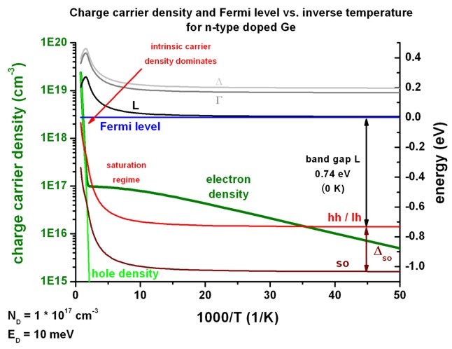
In a perfect semiconductor (in the absence of impurities/dopants), the fermi level lies close to the middle of the band gap 1. Fermi level of metal and semiconductors: This is the paper that pointed this out: The value for the fermi energy and carrier density is obtained at the crossing (indicated by the arrow) of the two black curves which represent the total positive and total negative charge in the semiconductor. Due to lack of sufficient energy at 0 kelvin, the fermi level can be considered as the sea of fermions (or electrons) above which no electrons exist.
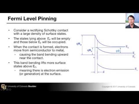
Surface States And Fermi Level Pinning And Metal Semiconductor Contact Youtube from i.ytimg.com Fermi level of metal and semiconductors: The fermi level is the surface of fermi sea at absolute zero where no electrons will have enough energy to rise above the surface. Green, unsw) illustrating the location of the fermi level e f relative to the valence and conduction bands for various materials. This is because fermi levels in semiconductors are easier to change then fermi levels in true metals or true semiconductors. The density of electrons in the conduction band equals the density of holes in the valence band. Due to lack of sufficient energy at 0 kelvin, the fermi level can be considered as the sea of fermions (or electrons) above which no electrons exist. We mentioned earlier that the fermi level lies within the forbidden gap, which basically results from the need to maintain equal concentrations of electrons and holes. 1.1 0, indicating equal concentrations of electrons and holes.
In the hypothetical case that the effective mass of electrons and the effective mass of holes are equal, the fermi level of a perfect intrinsic semiconductor would be at the center of the band gap.
Especially in complex compund semiconductors (like oxides and nitrides). (a) fermi level position in pure semiconductors at this point, we should comment further on the position of the fermi level relative to the energy bands of the semiconductor. The fermi level is the energy separating occupied states of the valence band from empty states of the conduction band at the absolute temperature t=0 kelvin. Fermi energyis the difference highest occupied state and lowest occupied state at 0k. For si withnd= 1015 cm3andni = 1010 cm3, using equation 3, ef nis 0.25evaboveef i. Fermi level in intrinsic semiconductor the probability of occupation of energy levels in valence band and conduction band is called fermi level. Fermi level lies in the midway between the valence band top and conduction band bottom of an intrinsic semiconductor, as shown in fig. The value for the fermi energy and carrier density is obtained at the crossing (indicated by the arrow) of the two black curves which represent the total positive and total negative charge in the semiconductor. However in 2003, it was shown that hydrogen has a universal energy level provided that the band gap of the semiconductor is aligned according to unified scale (for example aligned with respect to vaccum level). At absolute zero temperature intrinsic semiconductor acts as perfect insulator. Fermi level is the highest energy level occupied by the electrons in the material at absolute zero temperature. The addition of pentavalent impurity creates large number of free electrons in the conduction band. The fermi level is at e / u = 1 and k t = u.
In the hypothetical case that the effective mass of electrons and the effective mass of holes are equal, the fermi level of a perfect intrinsic semiconductor would be at the center of the band gap. Fig.2.7.2 graphical solution of the fermi energy based on the general analysis. In electrical insulators and semiconductors, the valence band is the highest range of electron energies in which electrons are normally present at. Each pentavalent impurity donates a free electron. This is the paper that pointed this out:
Fermi Level In Intrinsic Semiconductor from www.physics-and-radio-electronics.com For the intrinsic semiconductor at 0k, The fifth electron of donor atom is loosely bounded. The number of free electron depend on the impurity atom added. The term fermi level is mainly used in discussing the solid state physics of electrons in semiconductors, and a precise usage of this term is necessary to describe band diagrams in devices comprising different materials with different levels of doping. The highest energy level in the conduction band filled up with electrons at absolute zero is called fermi level ad the energy corresponding to the fermi level is called fermi energy. Energy level of conduction band consists of the electrons which are responsible for conduction. The fermi level is the energy separating occupied states of the valence band from empty states of the conduction band at the absolute temperature t=0 kelvin. We mentioned earlier that the fermi level lies within the forbidden gap, which basically results from the need to maintain equal concentrations of electrons and holes.
The fermi level lies between the valence band and conduction band because at absolute zero temperature the electrons are all in the lowest energy state.
Ec is the conduction band. If you can bring the fermi level high enough, then part of the tail will go over to the conduction band. About press copyright contact us creators advertise developers terms privacy policy & safety how youtube works test new features press copyright contact us creators. These electrons jumps up from the valence shell and becomes free. Fermi energyis the difference highest occupied state and lowest occupied state at 0k. 1.1 0, indicating equal concentrations of electrons and holes. The fermi level is at e / u = 1 and k t = u. The highest energy level in the conduction band filled up with electrons at absolute zero is called fermi level ad the energy corresponding to the fermi level is called fermi energy. However in 2003, it was shown that hydrogen has a universal energy level provided that the band gap of the semiconductor is aligned according to unified scale (for example aligned with respect to vaccum level). The fifth electron of donor atom is loosely bounded. Green, unsw) illustrating the location of the fermi level e f relative to the valence and conduction bands for various materials. Fig.2.7.2 graphical solution of the fermi energy based on the general analysis. (a) fermi level position in pure semiconductors at this point, we should comment further on the position of the fermi level relative to the energy bands of the semiconductor.
This is the paper that pointed this out: fermi level in semiconductor. Position of fermi level in extrinsic semiconductors • here the situation is different due to impurity of trivalent and pentavalent.


0 Komentar